Using a Balun for Current-Based Side Channel Attacks
By limpkin on Tuesday, October 31 2023, 17:19 - My Projects - Permalink
 Or how to use a common component for a completely different purpose!
Introduction
For several months, I had the chance to share an office with a security researcher whose hobby was to break the ESP32 AES engine by only looking at its current consumption.
His measurement setup was not ideal: long wires, a noisy current probe that required lots of trace averaging to measure anything... something needed to be done!
Why a Balun?
There are obviously many different tools to measure the current consumption of a given device: differentials probes, current probes, shunt resistors, LISNs... so why go for a balun?
The answer is fairly long and I actually was invited to hardwear.io to talk about this:
... but in short, the "standard tools" made to measure very small currents are either too noisy or don't have enough gain.
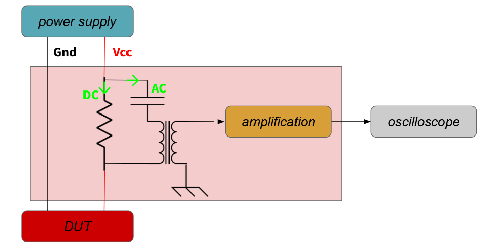
I therefore came up with the above concept which uses a balun to provide isolated current measurements: the balun primary/left side is isolated from its secondary/right side!
This effectively means that you can place this device on the Device Under Test (DUT) "high side" (on its power supply rail) or on its "low side" (between the DUT and its ground) as the amplification output ground is floating. On top of that, having an isolated output prevents ground loops, which could have introduced noise at our input!
The only downside of baluns is that they don't handle DC well, which is actually perfectly fine for me as side channels attacks only care about frequencies above 2MHz.
In the above diagram, DC current will go through the shunt resistor while the AC current will go through both the shunt and the balun.
Figuring out the details
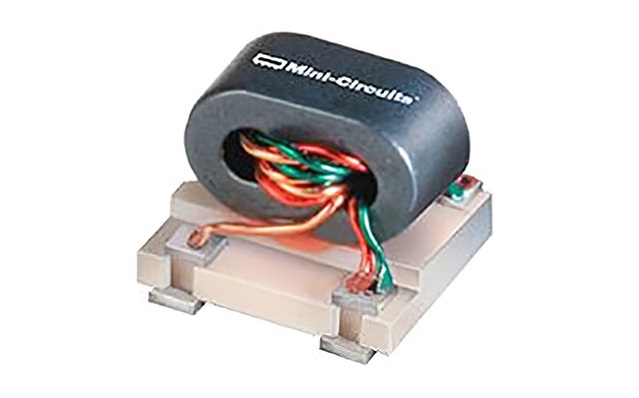
With the concept locked in, I started looking online for baluns. One important thing to know about baluns is that they expect a given impedance on both their primary and secondary side, and that impedance typically is 50 ohms.
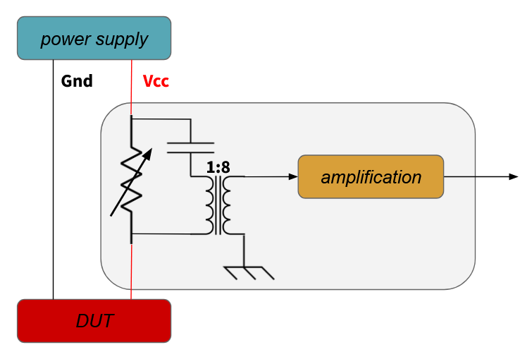
Luckily, I ended up finding a balun with a 1:8 impedance ratio, meaning that for a 50 ohms present at its secondary/right side, a 6.25R ohms impedance is shown at its primary/left side... quite the perfect value for an AC shunt resistance!
And what better component than a potentiometer to vary both the DC & AC shunt resistance to adjust the overall current to voltage gain?
But what about that "amplification" box? What should we use to amplify the signal coming out of the balun while presenting a 50R impedance at the same time? Given the balun stated 2-500MHz bandwidth, the answer was fairly obvious: RF amplifiers!
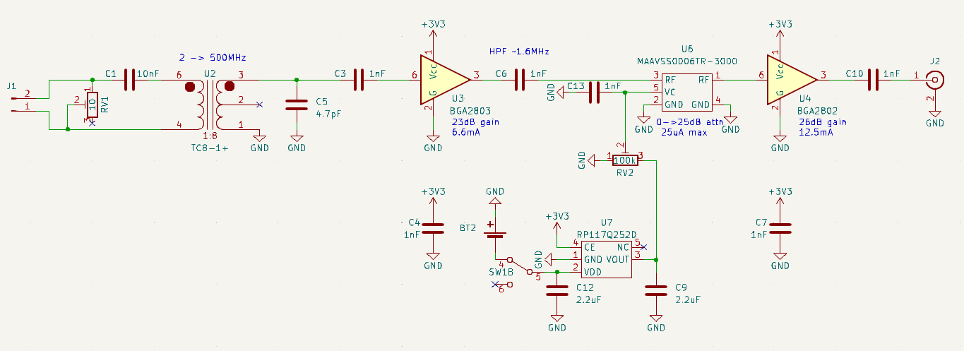
The amplification chain schematics
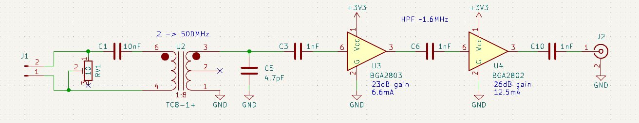
How apparently simple are these schematics?
You'll notice that I'm using two low noise RF amplifiers in series to get lots of gain... maybe too much actually!
For a 10R potentiometer position, the expected current to voltage gain is 50.5dB or 335x.
You may also be wondering why C5 is here. Well it turns out that during my initial tests I would get oscillations at around 2.2GHz because my amplification chain output would wirelessly couple into my input! C5 therefore reduces the balun's bandwidth (yup, it can transmit more than its specified 500MHz, likely due to capacitive coupling).
What provides power?
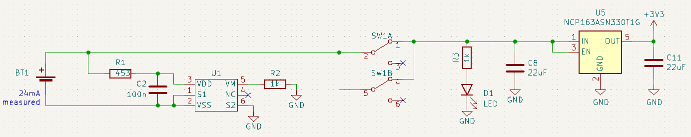
From the previous paragraph you'll have noticed that only a single 3V3 rail is needed to power the two amplifiers.
Using an external power supply was an option but just to be extra careful and not bring its noise to the board, which could then couple into our signal I opted for a lithium ion battery instead.
U1 takes care of its under/over voltage protection, and its 3,6V-4,2V output then gets passed to a 3v3 LDO.
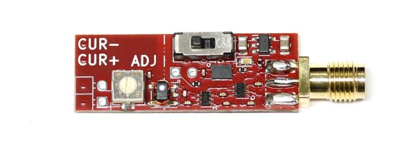
The final board
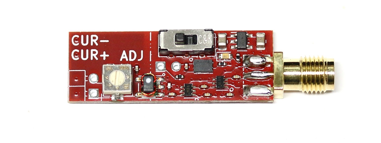
It is pretty small! Notice the two holes on the bottom left, to either directly solder wires or a standard 0.1" header.
Measuring the transfer function
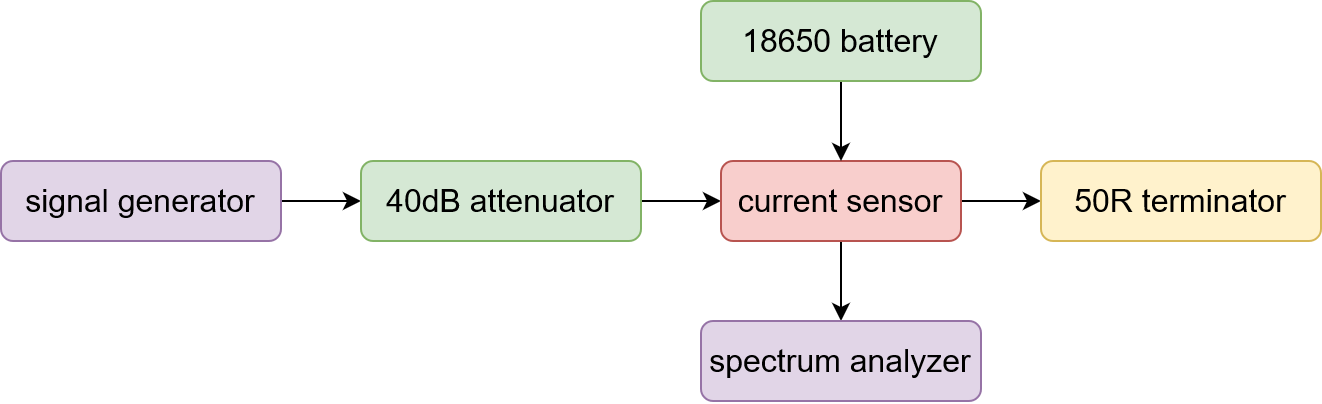
The transfer function was measured using the above test setup.
![]()
Looking at the above frequency response for different potentiometer positions, "gain flatness" are the two words that come to mind.
In that DC-50MHz sweep the gain keeps increasing.... which is actually fine for two reasons:
- actual wiring setups will heavily attenuate high frequencies
- side channel attacks don't care about frequency profiles!
...and that's actually lucky for us, as gain isn't particularly flat above 50MHz either:
![]()
What's cool in the above plot is that RF transmissions seems to be picked up at around 780MHz and 915MHz!
Keeping in mind that I'm using 40dB of external attenuation and that my AC shunt resistance is around 6R, for a 10R potentiometer position my expected overall measured gain should be:
20log10( (4/50) * (10/16) * 6) + 23dB + 26dB - 40dB = -1.45dB... which is fairly close to what we measure!
Improving the board by adding variable attenuation
Happy with that first board, I then decided to add a feature requested by my office-mate: variable gain.
I therefore found a very neat variable attenuator that only needs a negative voltage between -3V and 0V to vary its attenuation by up to 25dB!
Unfortunately that meant adding another battery to the board to provide a negative voltage... and a negative LDO so the set gain doesn't change as the battery depletes. As the current needed by the attenuator is extremely low, I'm using a CR1220 coin cell battery, directly inserted inside a holder located at the back of the PCB.
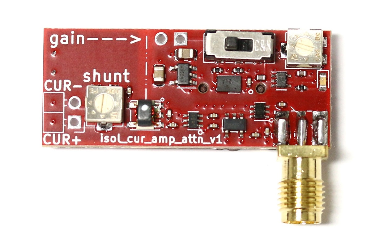
As you can see, the updated board is fairly similar to its first version!
![]()
Above is the transfer function for different set shunt resistance values and different attenuations... that's quite the range!
Does it work? The conclusion
It does!
The board is currently being used by several security researchers out there and ICs have already been broken with it!
You may find its source files here.
The boards are also available for sale:
- the fixed gain version: EU & US shop
- the variable gain version: EU shop / US shop
