My Business Card v2
By limpkin on Sunday, June 15 2014, 17:54 - My Projects - Permalink
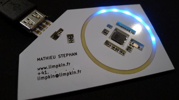
At the end of this month, I'll be leaving my current job. I therefore thought it'd be a nice occasion to build a new business card for my future interviews:
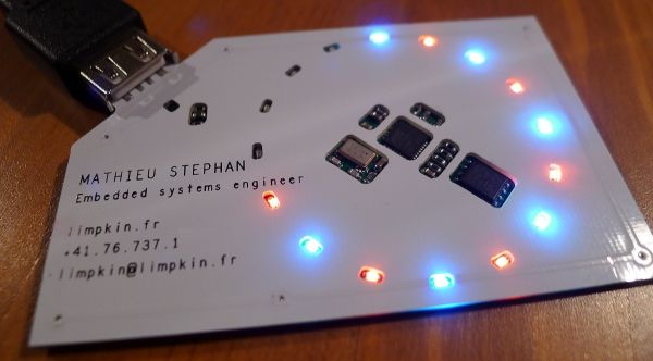
You may remember the first version of my business card made more than one and a half years ago (time flies!). It was basically made of two PCBs soldered together :
So why not simply assemble more of them? Well I wasn't completely happy with the way the two PCBs were assembled and wanted to try a new technique I had used for the top PCBs of the Mooltipass project:
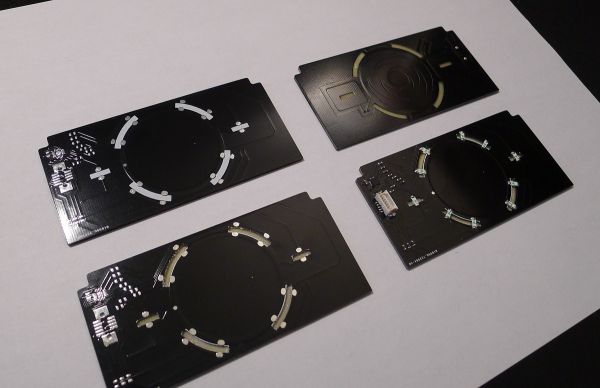
As you can see the PCB was slightly milled so reverse mounted LEDs may be directly soldered on the board. Well for this new business card the only difference is that the LEDs are soldered on the bottom PCB:
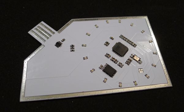
The new card stackup perfectly fits into a USB connector as it is 2.4mm high (1.6+0.8). The old version was actually thinner so I had to apply solder on the USB pads, which was not so pretty in retrospect. You'll be surprised to know that the new card can still fit in a normal wallet as it is completely flat.
However, the hard part was to solder the two PCBs together as a 1.5mm wide exposed copper 'band' was put near the cards' edges to this goal. Using a reflow oven with the card facing up turned the soldermask yellowish so I ended up soldering them by hand with a hot air gun.
Schematics and functionalities
Pratically nothing changed between the new and the old version except the number of PWM channels. I therefore decided to switch to the ATMega32U4 from Atmel (quite costly I know) as I could re-use all the code I had made for the v1. The card is still recognized as an external USB drive (2MB!) and can be reprogrammed via the integrated bootloader (launched by sliding some aluminium foil on the 3 exposed pads on the PCB shown above). You may also have noticed that the flash isn't exposed to the outside as I wanted to keep some kind of central symmetry.
I migrated the old schematics and layout to Kicad :
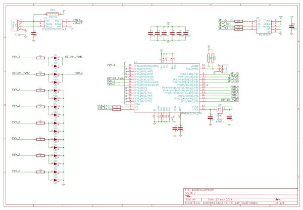
For a detailed schematics explanation and performance analysis, please head out to my card v1 blog post. The only thing worth mentionning here is that given the ATMega32U4 only had 7 PWM channels I had to use a given PWM channel complementary output and two extra I/O pins to enable/disable these given LEDs. Two groups of 2 LEDs will therefore always have the same duty cycle.
End result and resources

Click on the picture to zoom :-) . Here are the files you'll need to make your own custom business cards:
Business card v2 final code Business card v2 kicad solution
Cheers!

Comments
Hi, Mathieu!
Surprising news about the change of the job. I hope you found a better place to work. Successes and good luck to you!
Question: how do You usualy calculate the value of C3, C4, C5, C6, C8, C10.
Thank You!
@Zuinc : Thanks! These are decoupling capacitors... rule of thumb is to put 100nF.
Definitely a nice improvement over v1. The diffused LEDs looks really nice. I have a couple of questions for you.
Why did you cover one IC (the M25PX16 I think) but not the others? Also, whilst the visible but protected components are a great idea, there's something odd about how they sit at the bottom of the cutout. I can't place my finger on how it could be improved but it just seems strange.
Do you use standard LEDs that are just mounted upside down or are they LEDs that are specifically marketed as "reverse mount" LEDs. These seem to be designed to sit on top of the PCB but shine light down through it. However, the more I look into these, the more confused I get!
@Fred : Thanks!
Why did you cover one IC (the M25PX16 I think) but not the others?
>> Just for fun... and see if the interviewer wonder where the flash is.
Do you use standard LEDs that are just mounted upside down or are they LEDs that are specifically marketed as "reverse mount" LEDs.
>> Just standard 0603 LEDs on the bottom PCB.
Very cool build! Thanks for providing such a detailed writeup and sharing your kicad and software source. Is the only difference between v1's BoM and v2's BoM the change in microcontroller?
@euphonistihack : thanks... yep!
Another quick question: When you say that the total stack size is "2.4mm high (1.6+0.8)", does that mean you used a PCB thickness of 0.8 for the bottom board and 1.6 for the top? I would think the thicker 1.6 would be the top board to give as much clearance as possible for the components mounted on the bottom board, but wasn't certain.
Thanks again!
@euphonistihack : (sorry for the late answer) the top board is indeed 1.6mm and the bottom 0.8
Really cool build! I hope you don't mind, but I'm trying to use your KiCad source to build one for myself, and hit a few snags that I figured I'd make you aware of. For one, it looks like there were a few changes to the BoM:
USBULC6-2M6, a 6QFPN should now be IP4234CZ6,125, a 6TSOP (that has a different pinout than the USBULC5) http://www.digikey.com/scripts/DkSe...
FB1 wasn't in the original board's BoM. I don't know a whole lot about USB circuits, but I'm guessing http://www.digikey.com/product-deta... would be a good choice (120 Ohm @100 MHz, 2A limit)
It looks like you're using a different crystal on this than the last one, as the crytal from the previous BoM is so large that it touches the pads for the decoupling caps on the new board when centered. Unfortunately, TXC doesn't make a smaller version of that oscillator, so I'm not sure what you used as a replacement.
For two, I feel like I'm missing something with the KiCad layout for the top board. It seems like there should be some kind of milling where the non-exposed components are. For example, over the flash chip, I realize that you didn't want it exposed, but if there's no milling there at all, the edge of the bottom board can't get flush with the edges of the top board. Similarly, for the LEDs on the ring on the bottom board, it seems like there needs to be half milling on the corresponding location on the top board in order to allow the boards to be flush. I'm used to working in Eagle as opposed to KiCad though... is there a way to specify partial milling (half the thickness of the board) in KiCad? Or did you just place the solder paste on the outer ring thick enough to make up for the height of the flash IC and the 0603 LEDs?
Thanks again for putting this all together!
@njneer : Thanks! Please do... it's open source ;-) . Oh right, I forgot to explicitly mention that the ESD protection chip was changed indeed. Your ferrite is indeed alright. The crystal was changed to a 3.2x2.5mm (from a 5x3.2mm IIRC).
The milling was 1mm deep so the flash & leds could be hidden. I can send you solidworks files by email if you want!