Easy-phi Project: Low Cost Dual Discriminators
By limpkin on Thursday, January 2 2014, 13:54 - My Projects - Permalink
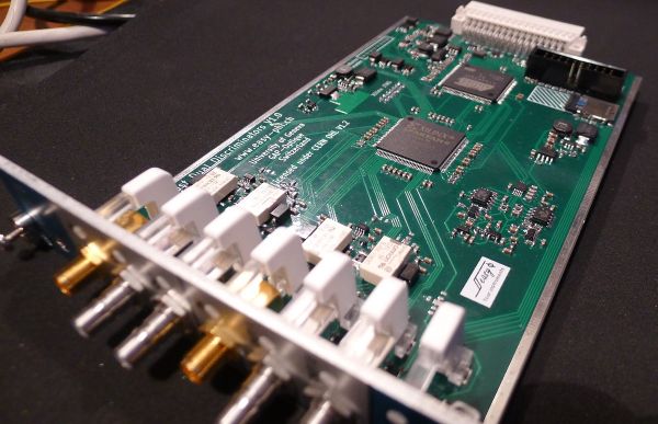
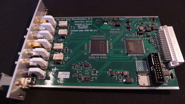
In physics experiments, it is often required to detect any kinds of electrical signals. That's why we developed this module:
Requirements
You may recall from my previous articles that easy-phi modules use a well-defined electrical signal to communicate with each other. Therefore, any easy-phi setup needs an interfacing card that converts signals from the outside to easy-phi compatible ones. Concretely, that means being able to detect pulses with different voltage levels and different impedances.
What's signal impedance? As you may already know, signals don't propagate well over long distances. The longer your cable is, the more diminished the high frequency components of your signal will be. That's why most bench tools offer a 50 ohm impedance mode, where the signal emitter has a 50 ohm output impedance and the receiver has a 50 ohm termination resistor to the ground. With this mode and the corresponding coaxial cables, a high frequency signal can easily be transmitted without being distorted too much (see signal reflection). In some cases, depending on the input signal standard, this 50 ohm termination resistor may be connected to another electrical level. This is what we call the input offset.
If you own an oscilloscope, you may also be familiar with AC and DC coupling. AC coupling is commonly used to remove the DC component of a periodic signal, aka the signal bias. For example, your audio card line input is AC coupled. This is done by adding a capacitor in series with your input, and is also convenient when signal references differs between platforms.
So how do these constraints translate on the electrical level? All in all, our discriminator needs to:
- apply an offset to its input stage
- switch between AC/DC coupling
- accept a wide range of input voltages
- switch between a 50ohm/high impedance input
- adjust its detection threshold over the whole input voltage range
Input stage
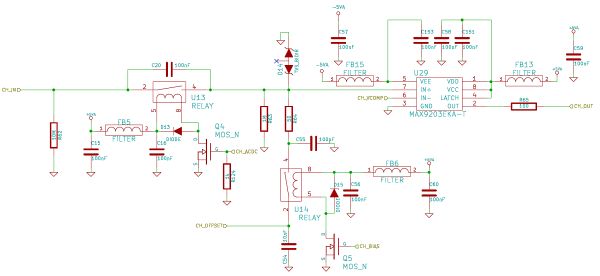
This is one channel input stage which uses two relays and one voltage comparator. In the picture above, the U13 relay is used to switch between AC and DC coupling (by shorting the coupling capacitor) while U14 enables/disables the input offset. These relays are controlled using N-Mosfets, and you can see that each one has a flyback diode at its terminals.
Component costs are usually proportional with their input bandwidth, which is why we designed this discriminator module to have a 100MHz bandwidth and therefore settled for the MAX9203 discriminator from Maxim. As a result, we can accept -5V to +5V DC coupled signals and 10V pulses on AC coupled signals.
When U14 is not activated, R64 and C55 form a 50 ohm termination for level transitions, which makes signal edges cleaner for high impedance signals. As usual, plenty of ferrites are used to filter high frequency parasites on the power supplies. On the schematics above ch_offset is the offset voltage, ch_vcomp is the threshold voltage at which the comparison occurs.
Voltage generation
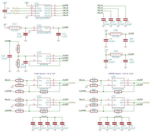
Obviously, we need to generate the offset/threshold voltages used by our input stages. That's why we used a 12bits DAC together with a 2.5V voltage reference and several operational amplifiers (op-amps).
Given we have -+5V power supplies and our threshold voltage has the same range, we carefully selected rail to rail op-amps having a high power supply rejection ratio. The offset voltage generation op-amps are different as they need to source/sink quite some current.
Input Logic
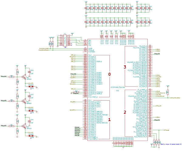
At this stage of the module description we can know if the input signal is above/under a given threshold. We now need to implement some logic on top of that: select the relevant signal's edge and either generate a small pulse or copy the input signal state to the output.
This is normally done with logic gates, but we decided to use an FPGA instead to give us more flexibility. We picked the spartan-3an which can be bought for less than $9. It doesn't have a lot of logic blocks but includes its own flash configuration memory.
An SPI interface is implemented between the FPGA and the main SAM3X microcontroller, allowing the latter to read/set different configuration settings but also reprogram the complete FPGA. This will allow future users to develop custom configurations that would suit their own applications. For example, we successfully tested a 100MHz counter implemented on the FPGA.
Each of the 4 outputs is made using one fast transistor and severals biasing resistors. The FPGA is also in charge of indicating input/output activity (by driving matching RGB LEDs) and send/receive synchronization signals via U44/U45/U46.
Conclusion
The total cost for this module is less than $200, which is quite acceptable for a device having these specifications. You may find all design resources on Github and if you're interested to contribute you may contact us at easy-phi[at]unige[dot]ch.
