Altium vs Cadence: a totally subjective opinion
By limpkin on Tuesday, July 17 2012, 20:17 - Others - Permalink
Let's imagine that, for some reason, you'd like to create a 4+ layer PCB, and that free tools such as eagle aren't enough for you (let's say for high speed PCB design or complex schematics).
You'd then have to choose between the two (but not only) major softwares available now: Altium Designer or Cadence Orcad Suite.
This is therefore my opinion about them.
(2012/07/23 edit: thanks to Graham and Dams for their precious remarks, this post has been updated with some additional infos)
First of all, let's emphasize the fact that this blog post is entirely based on my experience only. Therefore, it will be purely subjective even if I'll try to define objective grading criterias for schematics/PCB tools ;-) .
It will also cover a very small portion of what these softwares can do, as I want to focus on the features you usually use the most.
To plant the background, I've already routed 30+ PCBs on Cadence Allegro, some of them being 6 layers. On Altium Designer, I think I've only routed 5 or 6 PCBs, all 4 layers.
First, I'll explain here my personal definition of a good software, starting with the schematics part.
Well, a schematics editor is usually not that complex. You trace wires, add some net labels, off-page connectors... basic things. However, things may get a bit trickier when it comes to adding your own components.
IMHO, a schematics software should provide an easy way to draw your parts, and a clear way to manage your component library, to stay organized. The rest (mutiple netlists, multiple properties, pin properties) are just a 'plus' in my opinion. If you are thorough, if you know what you're doing and if you have a clearly defined way of proceeding when doing every single project... well you may choose to not even use them, choosing your own personal method to do without.
A friend of mine is a big fan of Design Rule Checking (DRC) that may warn you from stupid mistakes you may have done (wrong connections, unconnected pins...). Well, I've never done any mistake that could have been prevented by using it, so I'll remain skeptical.
As for the whole 'I have a huge pre-existing component library' argument... well I don't buy it. It never takes me more than 3 minutes to draw my own parts, and even if the software already had the part I would spend one minute checking it (right package, right pinout, etc etc...).
However, I am way more demanding when it comes to the PCB part.
A PCB routing software should be easy to use (o rly?). To define that subjective criteria, I'd like to propose here a simple 'easiness measurement metric' defined as number of clicks + number of keystrokes + mouse moving distance to perform a given function.
Why? Well because a good portion of the time you spend routing your PCB (time is money) is the time taken to perform simple actions. When you have to click 5 times, move the mouse 5cm to the right and 4cm to the left to do a simple thing, and you have to do this simple thing one hundred times on your PCB... it can get pretty long and frustrating.
Obviously you can design your own keystrokes for some (but not all) of the software functions. On Altium, it is actually very easy (either hold Ctrl + double click on the function you want to assign a shortcut to, or go to DXP > Customize).
A PCB routing software should have all these neat little functionalities that make visualizing your schematics from the layout in front of you easier. Obviously, having 2 screens when routing a PCB is for me a must.
I actually have three screens at home (two horizontal and one vertical) in this configuration: schematics > pcb > datasheets (and chats ;-) ).
The software should also provide utilities to display only what you need on the screen, and no extra stuff that would mess with your brain processing. Things should be clear, simple.
For example, why is Altium requiring me to display the layer I want to put a trace on?. If I just want to make a simple strap and I know there is nothing on the other layers, I really don't need to spend time switching views...
As for the schematics part, database management is also a very important part of the PCB software. I personally want to be sure where all my components are located.
On this topic, Altium and Allegro do things differently: Altium has a single file containing all the footprints of a given library, whereas Allegro create a single file for every component and pad. Being a maniac and a perfectionist, I prefer the Allegro way.
So let's start the comparison.
Allegro vs Cadence
First, you have to know that I've followed a eagle > allegro > altium > soon cadstar trajectory. So I am/may be biased :-D .
As I didn't find any huge difference between Cadence Capture & Altium schematics tools, I choose to only focus on the PCB part. In my opinion, this is the part where there is a real difference between the two software suites.
The visual aspect
Let's set the scene. You're about to spend several days on a very complex task that is going to use all of your brain (well, only if you have size and cost constraints obviously). You'll be spending all this time looking at your screen and your eyes will inevitably get tired.
I personally set all my PCB softwares background black and work in a low light environment. I find it quite resting and allows me to relax.
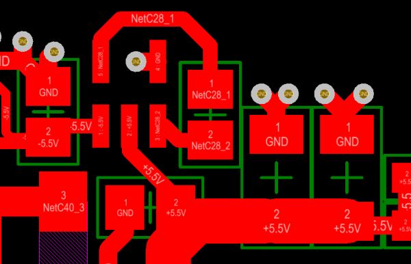
I need to be able to identify my schematics nets quite easily. Altium directly display the net names on the traces and component pads.
While on Allegro you need to leave your mouse on the component/net/pad/trace to know what it is.
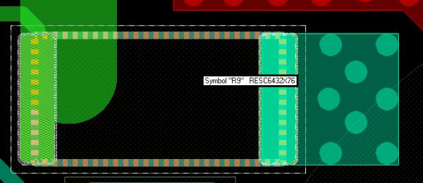
I actually think that both methods are good, as I always color my power lines because I route them last. Concerning the high speed signals, I usually route them first so I really don't need to be reminded all the time where they are.
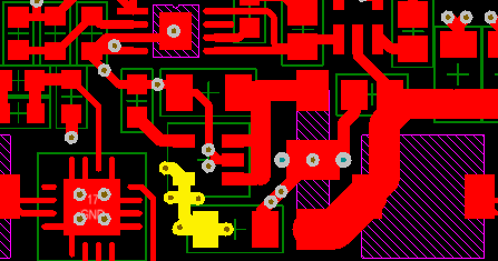
This is where Altium and Allegro differs: net colouring. For Allegro, it is quite easy: pick the tool, choose the color and apply it to the net. This net will then have its color completely changed.
When you do the same on Altium, on a zoomed out view it looks the same:
But when you zoom in, things look quite different:
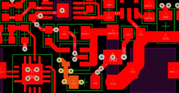
Edit: this can be changed by going in the DXP > preferences > PCB editor > Board insight color overrides menu.
Most of the time, I only display one layer at a time when routing. On a 4 layers PCB, first layer is for signals, second for GND, third for power supplies and the last for the remaining signals. On a 6 layers PCB, the 2 additional layers are usually dedicated for vertical / horizontal buses.
As a general rule, you want to optimize as much as you can your first layer use.
Anyway, both softwares provide a 3D view of your circuit, useful when creating your enclosure box.
On Altium, you can even route in 3D, but I seriously think it is pointless. By the way, Altium 3D view is much better than Allegro's.
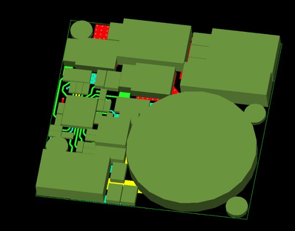
I also fail to see the point of having a nice 3D view, except to attract clients with shiny pictures displaying your know-how. A rough 3D model of your board is more than enough for the mechanical guys ;-) .
The views
I always create personallized views of the PCB i'm working on.
Sometimes I just want to display the board copper in order to maximize the space between the traces, and sometimes I just want to display copper + packages keepouts to put all the components as close to each other as I can.
On Altium, the 'easiness metric' result for this function is way higher than in Allegro. You need to click on the bottom left of the page, click on the top left of the popup window to select the view, and finally click on the bottom right on OK.
In Allegro, things are much easier:
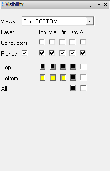
This panel on the bottom right of your screen allows you to switch on the fly between your stored views (.color files) and the generated gerber views. How cool is that.
And if you don't want to use this little menu, you can also click on the little boxes to choose what you want to display.
The filters
The what?
Let me explain here. You usually don't want your PCB software to behave the same way throughout the entire routing process. Sometimes you may want to only move/stretch/ripup/delete traces, sometimes components, etc etc...
On Allegro, you have this very neat little panel on your right that allows you to apply a filter:
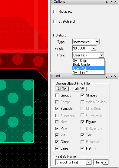
This way, you'll only be able to click on the filtered elements. This allows faster mouse movements as you don't need fine mouse control and thus provides you a better routing performance.
On Altium, it is +/- inexistant, as it has a smarter filter tool that allows you to build queries to select/modify parts of your design.
Great if you want to spend a few minutes building your query (depending on how long you have been using Altium).
Let's talk about how you know what you're going to click on.
Allegro higlights the element it thinks you want to select. Simple and logic right? However, it may require you to do some fine mouse movements to precisely point to the right element.
Altium asks you every time what you want to select if there's more than one element around your mouse. This leads to this:
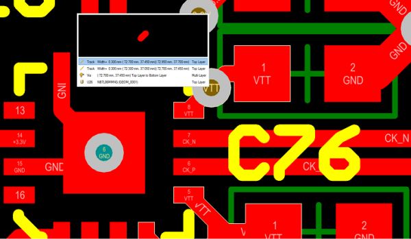
So my mouse is right in the middle of the via, i'm double clicking, and this pops up every f*cking single time.
Master, do you want to choose the via, the part, or one of the two traces around it? Major facepalm here.
One additional thing that may be useful: the ability on Allegro to quickly switch the way you move your parts: either pick it up from symbol origin or from the user pick.
That means choosing between one or two clicks to move your component. Sounds stupid, right? Well, very useful to do either fine or coarse positioning.
The debug
Ok, this blog post is becoming weirder and weirder
I don't know if this already happened to you, but sometimes I fear that the software has done something to my routing and I have no idea what.
I also like to see what the software understands for everything that I do.
Allegro has just the thing:

Yes, a console. You can even enter your own commands in it! Redefining keystrokes on the fly, seeing debug messages... it is actually perfect for a geek like me.
Putting traces on your board
Altium and Allegro have two complete approaches here as well.
Allegro checks that each end of any trace is properly centered on the destination pin/pad. while Altium just checks that the copper is just touching it.
In my opinion, this encourages easy routing and neglecting proper connections. But it is not that important anyway.
Let's talk about Altium's stretching algorithm.
Let's say you have this via:
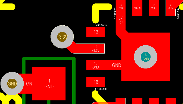
And you want to strech it to the left:
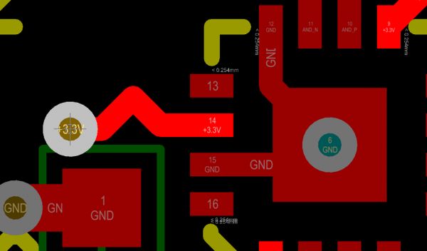
(Edit) By default, it is quite annoying.
Luckily, this can be changed by going to DXP > Preferences > PCB Editor > Interactive Routing > Set "Routing Gloss Effort" to Strong.
Allegro has the correct behavior by default.
Something I also wanted to show you. As I told you, I only display one layer when routing in Allegro:
Let's say I want to add a via in the center and I have no idea what's under:

Not only Allegro shows the bottom trace I'm disturbing, but it is also doing the proper changes to it. Nice feature right? (I swear I'm not sponsoring Allegro here).
The conclusion
There ain't any.
As I told you, this is my personal opinion only and I'm sure that if you have actually read this post ;-) you'll understand what I prefer.
People route in many different ways and I'm not saying mine is the right one.
For information, I have been told that Allegro's license is currently cheaper than Altium's.
It is also worth mentionning that this article is a bit useless if you aren't an entrepreneur... when you come to your job, I don't think you have a choice on the tool you're gonna use :-D (well, except at mine!).
(2012/07/24) The conclusion of the conlusion
After being featured in Hackaday this post has created a lot of reactions.
First, thanks a lot to all the people that pointed out the details I didn't know about.
Obviously, I have a better knowledge of Allegro than of Altium. So I could say more things about what Allegro had that Altium hadn't rather than the other way around.
However, I think that everyone will agree if I say that both software suites are comparable in the sense that there are no important tools that are missing in one or another. It's a matter of preferences.
Still, there are a few things that will make me prefer Allegro: smarter rat enabling, better debugging, user component placement when going from the schematics to the PCB, faster filters, absence of this annoying popup window ;-) .
That's all folks!


Comments
Thanks for the informative comparison. I use ExpressPCB for my designs but unfortunately you're limited to buying your PCBs from that company only. I wish someone could make a program similar that saved in Gerber formats.
Nice post, very interesting.
I have a comment about the 3D view, I think is more for design a case for the product than to attract client with fancy pictures.
I have been using Altium nearly every day for the past 5 years on 4-22 layer boards and I find new "features" about once a week.
Nearly every complaint you had about Altium can be fixed or changed in some manner.
For example - you can change what net coloring looks like up close AND far away. You can change whether there is a color pattern or a solid color, etc.
All of that to say: Altium's feature list is so vast that it is a huge hindrance to new users.
The basic version and pro version of the Cadence tool is now a fair bit cheaper than Altium. For large and high layer count PCBs Cadence is the better option . IMO Altium has a nicer schematic tool but for pure PCB layout Cadence is without doubt a better tool plus you don't need a super computer to run it.
For hobby use I personally think EAGLE is a great package.
I think you brushed over the awesomeness that is Altiums 3D capabilities. You can export the entire board with components and use it to build a case in another software. Or you can even import a case into Altium and design the board to fit it. It even does collision detection of the board, case, and components.
It is funny though that a lot of the stuff you mentioned negatively about altium is what I liked over allegro. really goes to show you how true a statement "to each his own" is.
Hi
Nice comments - I'm a heavy Altium user but am always looking out for other options. I might give Allegro a spin some time.
I'd just like to add to a few of your comments on Altium - not to start a religious debate or anything, as I do agree with a lot of your negatives about Altium...
The 3D modelling in Altium is fantastic. Yes, routing and moving parts in 3D mode is pretty stupid. However, you can bring in models (such as your proposed enclosure) and see how well your PCB fits. This feature has saved me many times - in the past mechanical fitment issues have been the reason I've needed to redo a board!
As for single layer mode - yeah some people prefer it, but I prefer the mode that grays out the unused layers - that way you can see if you are about to place a via under a heatsink or track over an area that you need to keep clear. That's my preference anyway.
But yeah, if you could set Altium to never ask you what you want to move and just default to the via, hell yes I'd like to see that!
Lastly, some tips on routing (if considering manufacture in volume):
1. Always enter the ends of component pads, not the sides. Prevents 'tomb-stoning'. Google it.
2. Keep trace widths sensible when entering pads. The big 5.5V traces you have in your first Altium screenshot will make nice heatsinks in the soldering process (if done by hand, you can just solder for a bit longer, but causes grief for automatic processes that can lead to bad joints). Use a 'fan out' rule to check for this.
I'm fairly new to PCB design, but have recently moved from Allegro to Altium at my work. I completely agree with you about having to clarify which object you want in Altium when it should be obvious - so annoying! I really like how integrated the Altium package feels, though; it's quick work to move between schematic capture, component design, and PCB layout. It always annoyed me in Allegro having to open up multiple programs just to design a new component (padstack creation, pad placement, schematic symbol creation). Having briefly tested KiCad, too, I was surprised by how many features it has when compared to the commercial products.
@AXT : Yep, I agree that it can be annoying. You'd then have to start your trace from the component pad directly. I have never tried this old Orcad actually... I was too young :-) . I also know professional PCB routers that have a huge set of shorcuts and scripts... very impressive!
@Graham : Really? I've asked several friends of mine before publishing this article to be sure that I was not saying erroneous things... Could you send me an email detailing the solutions for each problem? I'd be more than happy to edit my post
@zlittell : It's true I skipped over this part a bit too fast... And yes... that's why I didn't want to draw a conclusion :-)
@Simon : I'll edit my post to talk more about this part of the 3D capabilities. Thanks for the tips! The capacitors where you see the side traces are actually 0603 or 0805, so i'm not sure a tombstone effect can happen here. This board was actually a single prototype, hand soldered for a very particular project at work. I route differently depending on the final application.
@Iain : didn't know that! I agree with your view :-)
Dude, if you think Altium is bad, then you have not even used a bad software. I work as a hardware design engineer and our company uses Mentor Graphics PADS Logic/Layout. Logic is okay... kinda. But Layout... Oh boy, that's just hell. Every day I bang my head against the wall because it's so dumb, un-intuitive and just bad. At home I like to use Altium (which I LOVE because it's so easy) and I have never tried Cadence packages so I can't compare. But you should really try PADS sometimes.
@Ron : Hey Ron, checkout FreePCB. I've been using it for years, prefer it to Eagle and KiCAD for most of my designs.
Hi guys,
We are looking into moving away from PADs (which sucks with the new frontend) to either Altium or OrCAD (which seems to be similar to Allegro you were talking about). We agree, that the 3D stuff is just shiny and we don't need to see a 0603 resistor in 3D. But the routing is the most important. So correct me if I am wrong, if you do 4 layer boards, you would suggest Allegro. We have mainly 4 layers and sometimes 8 layers for FPGAs and it is tight all the time, so I like OrCAD's Constraint Manager for all differnet spacing rules we have to follow. Does anybody have experience with a little complex rules in Altium? I only saw that this is formular based for each net and part of a net, when you have a series resistor. Is this really the only way?
Thanks for comments :)
Jim
Hi Limpkin and all others
I m working with Altium Designer since 7 years in both schematic and PCB environment and I have to say that I m not totally agree with your description of the Altium Designer capabilities.
1) The first point where I was surprised was of course the customization of the editor, you can add your own shortcut in a very easy way. Just hold the Ctrl key and double click the icon/menu entry you would like to edit, then give the shortcut key you want and press OK, job done!
2) It seems that you are lot in trouble with the view in the PCB editor, actually you don't need to enter the view configuration dialog every time you want to enable/disable layers, you can predefine Views with the Layer set feature. Click "LS" at the corner left bellow of the editor to choose predefined views of layers, or you can create your own set and can be changed quickly with shortcuts.
3) Concerning the color override, If you don't want that the color gets marked with square when you zoom in, then just display it as solid. You can do this in the Preferences>>PCB editor>>Board insight Color override.
4) You think 3D is useless? That's the future of electronic design, the ECAD and MCAD world are communicating together more and more, having the ability to export or import the 3D to check if the board with the component will fit the case is just a revolution in the right way and not something useless, the most of the engineers will agree with me at this point.
5) Now filtering... no existent you said? Actually I use the Filter panel of Altium Designer every days, it looks different than Allegro but you can easily create the syntax you need to filter objects, then If these filtering are used often, you may pick them up in the history menu of the filter or even better, you can create your own favorites!
6) Concerning the Pop up dialog that appears when several objects are under your cursor in the PCB, I agree that this has been annoying at the beginning of my work but there are different way to get ride of it.
Here again the layer set is going to help you, if a layer is not visible then the objects of that layers are not poping up. In the same way you may use the "Single Layer mode" by pressing Shift+S, this is the view of one single layer.
Or the third possibility I know is to lock the objects, in that case they will never pop up in that dialog.
7) Now the routing engine, Altium Designer offer different capabilities for the routing itself but also when moving existing routed objects.
If you look in the properties of the dragging/routing engine you will find a gloss effort settings that keeps the angle of the tracks when moving them. I think you don't know this (according to the picture I saw above).
Actually after reading you article I had directly the feeling that you are a good cadence user but by Altium Designer there is still things to learn.
When we bought our Altium Designer license we order a Basic Training as well. This was for me the perfect way to learn the basic things, I've also learn some more tip & trick on the forum, the community of the users is very likely to help new customers.
P.S. I don't want that you take this personally, this is just to show to the other engineers that Altium Designer is a fantastic Software, and I have to say, my favorite one!
@Dams : Don't worry, I don't take it personally :-) . Thanks a lot for your comments, I just edited my post accordingly!
A few points I wanted to clarify:
- I only said NICE 3D was useless. I mentionned that 3D was very useful for creating enclosures
- I didn't say that filters were inexistent... I said you need to spend quite some time learning Altium syntax to be time efficient
Cheers
Hey guys!
The post has been rewritten to be more "politically correct" and to incorporate the few details i wasn't aware of :-) .
Cheers!
Hi guys and gals, thank you for the exchange of information. I've just done my first semi-complicated design in Altium. I find it far more capable than the 15-year-old OrCAD I used in prior life (company too cheap to ever upgrade), but also somewhat scary. I guess perhaps I'd be less scared once the boards come home and there are no errors in the copper, but for now I'm wary.
The wariness in using Altium comes from what seems like just dancing on the edge of logic flaws, and the relentless pace of updates that render Altium's own documentation useless. Let me explain what I mean on two examples. I'm not talking about the user interface or productivity side of things, not about how long it takes to do a task; I'm talking about whether the copper comes back and it's working the way you think it should, and the way the tool told you it would.
Here's the first: plane layer logic seems close to broken in Altium, on a conceptual level. I didn't find that out until I was too deep into the design; had I known, I would have just used positive copper and polygon pours, which so far appear nearly logic-flaw-free. The fault: The plane clearance rule is unary, and it should be binary. So, say I have a moderately high-voltage design. I would like to have a default clearance, and then a larger clearance for my high-voltage tracks so they don't spark. If I have high-voltage vias going through a plane, they clear with the larger standoff distance; all is fine... until I get a portion of a plane that itself is high voltage.
Then, there appears to be simply no way to tell the tool to enforce larger clearances with respect to this portion of the plane because the logic, with all of its magnificence of a hierarchical set of rules, doesn't allow for this kind of requirement. You can manually draw lines around the high-voltage split plane to create a larger standoff with respect to other split planes on this same layer, but low-voltage vias through this high-voltage plane still draw with the smaller clearance—the rule for plane clearance is unary, not binary. It seems that neither online nor batch DRC would have flagged violations resulting from this "feature"... I know; don't use planes to carry high voltages, this tool ain't rigged for it. Lesson learned. The question is, what other monsters lurk in there?
Perhaps if you're 5 or 7 years into Altium, you'd have enough confidence to say "a vanishingly small number", but for me as a sole engineer at a quickly moving company that is not particularly inhibited by resources, the risk of using a tool with at least one seemingly profound flaw appears large enough
to seriously consider switching the tool. I'd rather lose a couple weeks learning how to be productive in say Allegro, than spend say a week on figuring out why my high voltage sparks on every single board when Altium's DRC tells me that can't happen, then two weeks on respinning the board, and then learning Allegro anyway because the management is about ready to lose faith in engineering's ability to design working boards.
Next, there is no such thing as a bug report with Altium. Assuming that my above observation is correct (and it may not be; perhaps there is some third way to do a DRC that would have flagged the insufficient plane clearance that I simply haven't found in my 4 months of active Altium use), there isn't a way to report this as a bug requiring action, or to receive a confirmation that it's indeed a feature and the suggested workaround is such and such. Altium currently doesn't accept bug reports, since they are apparently so overwhelmed with past reports that fixing them is what they are working on. There are other flaws of about the same level of meaningfulness that I noted in my early use; I was very happy to note them fixed in the releases of the past 2 or 3 months, so perhaps the future is bright. But, the lack of a bug report mechanism—and we are paying $$$$ for a subscription—does nothing to inspire confidence in the tool.
Next and last, Altium's own documentation doesn't seem to keep up with their updates. For example, I spent about half a day trying to figure out how to display design violations in a succinct way, other than the batch DRC. RTFM doesn't help; Altium's own documentation uniformly refers to Rules and Violations drop-down menu item of the PCB Panel, but there isn't one. Users on various forums seemed to be just as puzzled as me. Turns out that PCB Rules and Violations is a panel in itself now, and it needs to be enabled by checking a box after bringing up a menu after clicking on "PCB" in the right-hand corner of the main window. There are at least a half-dozen other items that are just like that—changes made to the interface, no changes to the manual. This isn't as critical as errors in the copper, but again do nothing to inspire confidence.
Thanks for reading, hope this was helpful to someone.
@vgusiatnikov :
You can enforce different plane clearances based on different criteria.
For example, on the simplest level, you can create a plane clearance rule based on a specific net, one that might be at a higher voltage level or the like. You could also create a whole net class called "High_Voltage" or something of the sort and set up your rules to pour a bigger clearance for that whole net class.
If you go to the rules section in Altium, right click on the "Power Plane Clearance" and select "New Rule", it will create a new power plane clearance rule. You can then use all of the criteria on the right side of the menu to determine what your clearances for a certain net, net class, primitive type, etc will be.
Again - after using Altium as much as I have, I almost never say "it isn't possible in Altium" so much as I say "I don't know how to do that in Altium." But you are right, it has a very large learning curve and if you are trying to just get the job done ASAP there are probably better tools out there.
Thanks Graham, but all plane clearance rules I may define are still unary. There seems to be no way to make a rule based on what the plane is, only on what the viaing net is. Of course I can overprotect myself and set the clearance to the max I would ever need, but then all of my planes would look like disconnected swiss cheese. Wouldn't this appear a problem?
I liked this discussion. I myself have been using Altium for some 5 years for pcb designs below 2.5 Gbps. I need to do a pcb layout which contains 12 Gbps serial differential interfaces. I've read in forums that Altium is not a tool that should be used for multi gigabit pcb design and they recommend use of Allegro.
Ref: http://www.eetimes.com/design/embed...--A-board-developer-s-perspective-
So from my perspective one comparison that is missing is how the two tools: Altium and Allegro compare when it comes to signal and power integrity analysis.
How does the two tools compare if lets say we need to design pcb having mutli giga bit serial differential interfaces such as Xilinx MGTs having signal rates touching upto 12Gbps. Is Altium not an option at all when it comes to designing pcb having say above 5Gbps interfaces?
I hope I am not dragging the discussion in wrong direction. I apologize if i did so.
Regards
Moving from PADS to Altium on my part was a pain in the @$$. There was a paradign shift to say the least. The learning curve was tooo challenging that I was learning Altium by myself referencing from forums. I design industrial boards (ATE) with 20-30 layers and we have design methodologies that are different to commercial boards out there. I was unhappy with the time it took Altium to repour my copper planes whether they are negative por positive planes. PADS do it in less than a minute while Altium does it 100x or more.
I won't recommend Altium at all even if it is of lower cost compared to PADS or Allegro. You get what you pay for, if you know what I mean.
Well i agree with most of you guys, Altium Designer doesnt have the ease of use of Allegro, Pads or Expedition PCB. I have used a few tools and i still prefer the Mentor graphics programs, too bad they are pricing themselves out of the market.
I would recomend Altium to people laying out motor controller pcb's and such, but the control you have over planes and routing isnt great so dont use it for designs where you need more control over routing like under fine pitch BGA devices. Altium has its market. Lets hope they work on updating their legacy dependant user interface.
Hello, Your blog is interesting and was a good read but there are some glaring ommisions with respect to Allegro that I would like to point out.
1 Setup time on Allegro is Horrible. The learning curve is difficult. To be productive on day 1 or day 30 with Allegro PCB editor is a serious stretch. The biggest hurdles a designer will face are.
Figuring out the layer structure of the entities that compose a footprint.
Defining colors for layers. BTW all your color settings get blown away if you do not
save them to a parameters file : )
DRC has endless settings.
Paths to symbols,Padstacks have to be defined otherwise a user will never be able to package a design from the schematic.
Basically everything in Allegro has to be configured out of the box where by competing tools have the basics covered and are easy enough for the end user to
know what button to push.
Allegro does not have any library managment Period. If a user wants to look at their PCB footprints they have to open the pcb editor and then open the .dra symbol. This can become a huge task because each "Symbol" is kept in a folder and not a database so a user has to open each symbol to just browse their symbols. BTW footprints are called symbols in Allegro.. That one is hard to believe :)
Padstacks are kept seperate too, there is a padstack utility to allow you to browse your padstacks but there is no "Preview" of what your padstack looks like.
Library management and padstack management are basically a Joke in Allegro.
Now putting aside the setup time involved with Allegro and some of it's weaker features it is a serious PCB editor. It can basically do anything but the price of admission is you have to take the time to learn it. Once you do it will be one of the best PCB editors you have ever used.
Allegro's strong points are. V16.5 X
High speed routing and net rules.
Interactive Routing.
Extremely Fast graphics Display. "Zero lag"
Shapes or the ability to create and merge complex polygons with ease.
Reports, such as net, bom, drc, Pretty much endless list.
Highly configurable "Comes at the learning curve price of admission"
Things that will drive you insane
No real nested commands. Assume you want to move a component and then route a pin. You have to select each operation to do each action. I..E move component then click add route. Other tools combine common actions such as this Allegro does not.
Configuring all the settings : )
Thanks for the useful blog and comments!
After starting many years ago on Protel, then moved to Veribest and now have been using Allergo for quite some time (Let's not confuse Allegro with OrCad layout, they're both Cadence, but completely different: Allegro works, but it is not cheap).
Now I'm moving back to Protel in its new form; Altium, and finding it quite powerful for queries and lists, but very annoying for it's clunky interactive routing engine. And yes, that pop-up which asks what you want to select is idiotic! Especially when routing under a big BGA it always asks if I want to move the BGA, duh! Plus a track should snap to the centre of a via, and I'm tired of deleting bits and pieces of track when I change something.
But here's the real gripe: I'm working on a DDR layout and have to lenght match the traces. Here there are often several chips on one address bus resulting in a "T", and you need to match each leg of the T. Allegro does this well with pin-to-pin rules and also allows inclusion of the Package Pin Lenght. Altium... well let's just say that I was very glad to find a video and spread sheet by 'Fedevel' showing how to do it (thanks for that Robert!), but again the process is very clunky. And when it comes to signal integrity? forget it!
It would be great if Altium left out the FPGA support stuff (we're going to use Xilinx's or Atera's own software for that!), and concentrate on good routing and high speed support...
@John Smith : It's interesting you mention that, because it is exactly what I love about allegro :). I like to know that each padstack/chip is a separate file on my computer that I can pick for another project.
Hi, I am a typical Altium user, but in last days i have the need to use also Orcad. So i had spent a lot of time to look it(I had started originally with very old Orcad, but then i migrated to Protel99 which was definitely better then). Now with Allegro i see Orcad had become much more user friendly, but yet i consider Altium for me more comfortable overall. Of course every program has small things we do not like, but things I do not like in Orcad are more.
From a "LONG TIME" pads user. The Altium toolset is now approaching the ease of use that pads has had for a long time. The 'new' version of pads is forcing many to step back and re-evaluate their tool sets. I see many using Orcad for schematic and Altium for PCB layout. Is that a route that any here have a comment on??
Limpkin, I dont mind too much that each padstack is in its own file. As a old P-CAD Dos user that is how it was done way back. The downside to this from the perspective of a new or seasoned user is. Each padstack has to be named so you know what it means for example 60R-33 which would be a 60 mil round padstack with a 33 mil hole, now thats not too bad for a throug-hole hole but for smd pads it can be a pain in the butt : )
Most of the newer pcb cad tools intergrate the creation of the padstacks with the actual footprint which makes for easy footprint creation but the downside of this is one might not be able to change a pad on the fly.
Someone mentioned earlier that the Orcad product is not Allegro, it is indeed Allegro. Same interface same everything except they have removed some of the high-speed rules from the lower end package that they call Orcad.
If you are new to PCB design Allegro may not be for you but if you look at most of the large boards such as computer mother-boards they are getting designed with Allegro or Mentor. Very few large designs are been designed with Altiumn IMHO.
The graphis sub-system in Altium cannot handle large copper pours, it becomes a pig.
If you are after graphics speed then the open Gl based graphics of Allegro cant be beat.
Thanks John
Hi,
I notice you don't mention diptrace in the above.
I run an electronics business and design aproximately one new product per month.
I have always used diptrace.
When I tried one of the tools you mention (I wont name it), I found it difficult to do the main design tasks: PCB routing and layout, 3D visualization. (It took me one hour to become proficient in Diptrace). I really enjoy designing electronics. And I find it frustrating when these expensive bulky tools force designers to think more about the tool rather than the design. So, If you have an hour spare, try to design a circuit and layout a PCB (1 to 16 layers) in diptrace.
Also do a rule check, you will find a quick and intuitive default rule check, that requires no time to setup.
Also,
Can I add a note on 3D view functionality and it's usefulness
I have used this feature (of Diptrace) to check the dimensions of a PCB in an enclosure (using Sketchup).
Also, it is a very valuable tool when designing for a customer, to show them the product in 3D.. using a free VRML viewer I can email them the 3D file and get feedback.
The 3D function of Diptrace is Low-tech and quick. Just how I like it.
However I do have to convert 3D component modules to VRML format first.
Over the past several years I've been exposed to Altium and Allegro. I got pretty good at Altium and have been able to either workaround or ignore the annoyances. i think it's getting too bulky, has too many FPGA and compiler features nobody ever uses, and doing simple things like copying/pasting/moving vias are annoying. I also ignore the 4GB of libraries since literally they have nothing I need, and it takes a few moments to create my own components. I don't want a "vault" or "my altium" or any of that. But in terms of just figuring stuff out, it's pretty easy. I could easily imagine a more productive layout experience, but I've mostly done smallish boards. Despite Altium's annoyances, its discoverability is really good and in keeping with my post-1995 computer interaction expectations. I was able to learn Altium from a few PDFs. Its polygon editing features are annoying, and it has plenty of other quirks, but overall I don't feel like a retard using it.
With Allegro, however, after several years of trying to *casually* learn the tool between endless meetings and other workaday interruptions, I still have no idea how to take an Orcad schematic and bring it into the tool. Seriously. The conceptual leap from standard Windows-based tools is pretty large. I don't "get" how the tool works. There are endless config files at each level of the tool, from libs, padstacks, "symbols", comps, dxf conversion files, idf, colors, palettes, filters, lists, etc. I really don't know what I'm talking about, but this is what I see, and is in many ways a metaphoric mimicry of the sounds I hear in a foreign language. In the same way that Charlie Brown's kitchen expertise is limited to cold cereal and maybe some toast, my Allegro expertise, after several years of exposure in which I hoped some knowledge would diffuse through my thick skull, is the ability to move and delete components, import an EMN file (oh, sorry, import through IDF menu, whoops, I shoulda known), then export to DXF, oh, wait, I need to set up a conversion file, click three buttons, and hope the version i have doesn't have a bug. PDF? Sorry, you need a separate license for that, asshole. In fact I can't usually tell the difference between a bug and my lack of knowledge or just an unimplemented or "teaser" feature they decided to add the menu. (BTW I had a similar hate-cadence experience ~10 years ago in analog IC design world -- lots of unimplemened menu items and interface (java/non-java) inconsistencies, as though Cadence loves to leave you blue-balled after paying through the nose for a polygon-pusher; where's the "automation" part). When I want to cancel a command (has anyone at cadence ever read the principles of stateless user interface design) I cannot just hit escape. I have to right click then pick either cancel or "oops". I mean WTF? This is a >>$10k tool suite. Even Microsoft of famed Clippy or Bob doesn't say "oops". Also there are many times when I'm trying to use the arrow keys to move around, and the console window just says "right right right right esc esc esc esc fuck!" The only out is to hit enter. I think this is the only tool in the existence of the planet that captures arrow keys and prints them out. Finally, it sucks ass with most of my wireless microsoft mice. No matter which direction I turn the scroll wheel, it always zooms out. Doesn't happen with all wireless mice, or with wired mice. Does any other tool figure out how to fuck up a SCROLL_EVENT? So although the Altium curve may be steep, it's not a brick wall like Allegro, with every waking moment causing me to want to throw the computer out the window.
So basically we have other board people do the real layouts, and the rest of us with lives to squander just take a look using Free Viewer.
And don't even get me started on LMTools....
I have to agree with what sonicsmooth says about cadence allegro i myself can't get Orcad to export any kind of netlist Allegro can import ( Logic ) I have a help request in about this and will probably get a timely answer in a couple DAYS !!
I am a 15 year PADS user. the library is easy and the decal editor is easy AND you can add or delete nets from the layout tool dangerous maybe but fast.
Importing DXF is also easy and putting it where you want on the layout and in the library is easy. One bad thing I don't know how to put holes or vias in a decal without them being a terminal.
I'm probably die before I get Allegro figured out
Your article is so interesting....
I think Altium is better for visual things and Allegro is better for dedicated tools to design advanced board i mean high speed boards.
For larger designs I use Orcad 16.6 (nicer 3D now with STEP model mapping though slow preview)! Yes configuration and component creation can take some time but once you have it figured out it...
For small projects I use Proteus 8.
Free tools:
DIPTrace is cool for small designs and very cheap for bigger paid versions!
For serial communications testing with micros - you can't beat SimpleTerm Gold Starter Lite (free) and paid for version rarely use.
Get the job done with the tool you are comfortable with depending on your task.
Greetings
I am fluent in both 2 software
The altium Multi Brdpy pcb sheet is faster and more accurately
Thanks
I've been using Altium (Protel, et.al) for 14 years and my biggest gripe is The Bugs! Many that have been around for at least 14 years. Altium seems to be a company, like Computer Associates and how Microsoft used to be, that is more interested in adding new features/bells/whistles than making a solid product. About every 10th time I start up the program something has disappeared or changed in the interface and I have to go hunting to recover it - when I do a re-annotate on the schematic and import to the PCB it looses track of tons of nets, recently - I run a DRC and it doesn't report any problems while there are still a bunch of unconnected nets (and yes, the DRC is set up correctly). I could go on and on and ...
If they just took the time to fix the fundamental bugs, fix a couple of architecture issues (e.g., losing nets after re-annotation), make the user / commands more orthogonal and intuitive, and provide better (not necessary voluminous) documentation and help search, they would have a great product.
Thanks for listening to my rant.
Doug
I've been using Protel and Altium for almost 18 years with a brief stint in Zuken. In the beginning polygon repours would take hours, by 2009 it only took minutes but still enough time to get a cup of coffee. In Altium 15 polygon pours are very fast. I have repoured every polygon on a 12 layer 8"x11" board in under 30 seconds.
As for 3D, since 2009 we have used a STEP model for every part in our library. By using an accurate 3D model and Altium's 3D engine we have been able to get real time 3D clearances during placement. I can place a small SMT component under a connector and know it will fit within my clearance rules.
3 minutes to draw a component? What about a large BGA component with hundreds of pins? I fail to see how you could draw that in 3 minutes. Also, the 3D aspect is very important. Have you ever had to do a thermal analysis or a frequency analysis on a PCB? It is important that the ECAD software can talk to MCAD. Even if you don't need that, do you realise how much better your designators are placed if you do it in 3D on Altium? I have no experience with Cadence and I'm not bagging it, I just think you make some broad brush statements in your analysis.
@matty : Hey Matty, about BGAs: actually less than 3 minutes as there are tools to quickly make such kind of footprints. After all you just need the grid size, number of balls and ball pad. I agree with you that on complex designs 3D is extremely important.
I am into my fourth month (yes months, not day or week) trying to get my first pcb layed out with 3D visualisations. I am the only one in our company working on Altium full time and hence I have to rely on forums and telephone calls to the local Altium office. The people at Altium have been very helpful but never before have I had to spend this amount of time on a package before I can see any reasonable results.