Using a Standard Coil for NFC Tag Implant Reading
By limpkin on Tuesday, October 7 2014, 11:53 - My Projects - Permalink
Who knew it'd be possible to use this coil to read NFC tags?
A while ago I backed the xNT campaign, which aimed at making an NTAG216 based NFC implant for different purposes. After a few months of waiting and a few weeks of trying to find someone in Switzerland willing to do the very simple implant procedure, I finally became a cyborg:
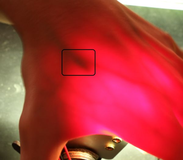
Sorry for the poor picture quality... it's indeed extremely hard to take one when you don't have access to an xray machine.
The implant can be read by most recent non-Apple branded phones and can be reprogrammed as many times as you want. It however only has 868 bytes of non volatile memory, which is actually more than enough to store my contact information at the moment.
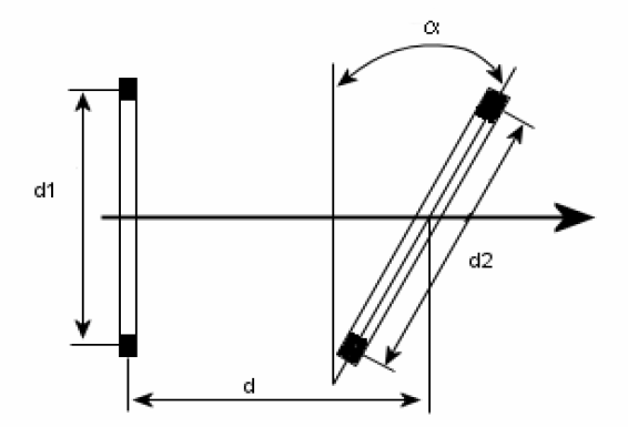
As your intuition may tell you, using a big antenna to read a tiny implant isn't the best scenario we can imagine. Most phones typically only have a small sweet spot where implant reading is possible. This is due to what we call the coupling factor that only depends on the reader & NFC tag antenna geometries and the reading distance squared:

From the equation above, it is obvious that our coupling factor will be maximum when r1 = d1/2 = r2 = d2/2. However, contrary to our intuition a coupling factor greater than 10% will cause several communication problems (see the PDFs at the end of this article). But we may not need to worry about that because of our reading distance (I have a thick skin) and the angle between our tag and the reader.
Conclusion? In a perfect world, our reader's antenna should have the same diameter as our implant's.
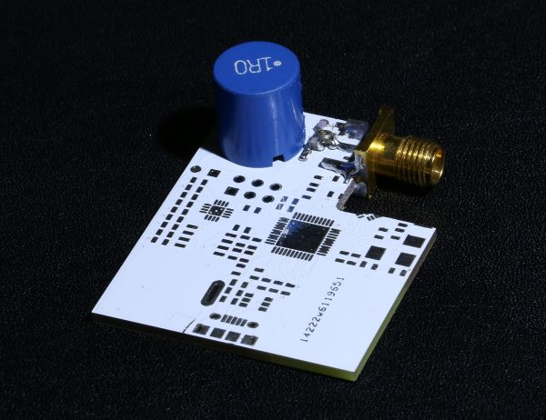
As I didn't want to wind my own antenna and thought that designing a small one on a PCB wouldn't be so convenient for hand positioning, I wondered if I could use a standard coil like the one shown above. This meant entering the wonderful world of antenna matching.
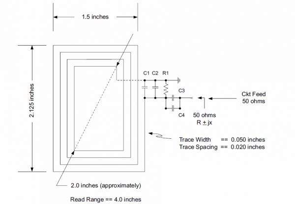
With a few hours of Googling you'll find many application notes containing standard PCB antenna designs. They're nice recipes you just need to follow to get a functional NFC reader in no time.
The passive elements you see in the picture above (C1/C2/R1/C3/C4) are here so the complex impedance seen at "Ckt Feed" is exactly 50 ohms. If your antenna circuit impedance doesn't match your transmitter's your power transmission won't be optimal.
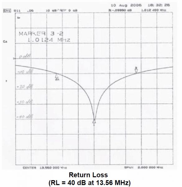
Power transmission can be checked by looking at an antenna's return loss for a given impedance (usually 50 ohms). An ideal case is shown above.
Note that the slopes around the 13.56MHz center point shouldn't be too steep as NFC ASK/FSK modulation creates other frequency components nearby. A typical 2MHz bandwidth is actually recommended to accommodate the upper and lower RFID sidebands for various data rates given in ISO15693 & ISO14443A/B.
This is called the antenna circuit quality factor, equal to F/BW = 13.56MHz/2MHz = 6.78 in our case.
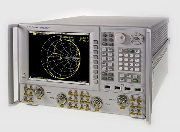
So how do we measure an antenna's return loss and devise an impedance matching for a non-characterized antenna?
We use a very expensive piece of equipment shown above called Vector Network Analyzer and some fancy software.
This machine will allow us to first know the complex impedance of our small coil, which then enables us to find the passive components values for our impedance matching network.
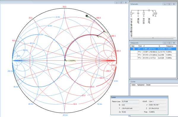
I used the free Smith software and a few applications notes to convert my coil's complex impedance to 50 Ohms. If you're interested in learning more about Smith charts, please have a look at the different documents at the end of this article.
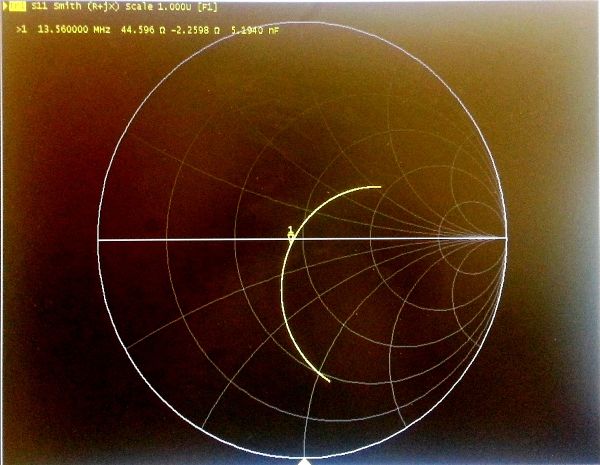
As you can see the final measured impedance isn't so far off from its theoretical value. This is mostly due to the passive components' tolerances.
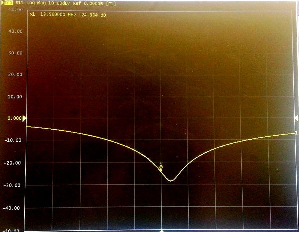
The maximum power transmission frequency isn't too far from our targeted 13.56MHz.
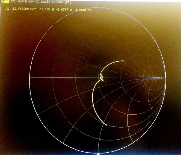
The smith chart had an interesting shape when my implant was on top of the antenna... which made me believe my idea could actually work. A few days later I purchased an NFC reader with an SMA connector (that I won't mention here because of very poor customer service) and actually managed to read my implant with it.

As you can guess, these empty footprints are here for a reason... but that'll be the topic for another article.
In the meantime, here are the PDFs I mentioned:
Antenna matching for the TRF7960 rfid reader 13.56 MHz RFID systems and antennas design guide smith chart fundamentals

Comments
Hello hello,
Très chouette article! (Merci de l'avoir posté sur hackaday, sinon je ne serais pas tombé dessus).
Apparemment tu as réussi à trouver quelqu'un pour réaliser l'implantation en Suisse. Est-il possible d'obtenir l'adresse?
That's a great project. I also have xNT implanted and found modules with smaller antenna are better for reading the implant (for instance ACR122T) than trying to find sweetspots in larger antenna.
Would be great if it was possible if thanks to this project you could shrink nfc reader or just antenna components and their tuning for them to be connected to the rest of the reader/microcontroler via wire.
ps. Hope it will be available for purchase at some point.
I'll be definetly following this project.
@Jean-Philippe Rey : Merci beaucoup! Pas de soucis, je t'envoies un email...
@Przemo-c : well, the current pcb is 35x45mm and has expansion capabilities ;)