Easy-phi Project: High Speed Logic Gate
By limpkin on Thursday, April 24 2014, 14:02 - My Projects - Permalink
Next in our Easy-Phi articles series is the High Speed Logic Gate board:
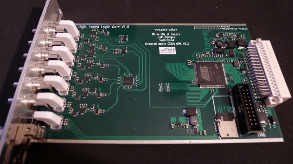
I'm sure you must be wondering why it is necessary to develop a complete card to implement such simple functions :-) .
Well, when you're dealing with high speed signals you unfortunately can't use standard cmos signals and therefore aren't able to just pick an FPGA/CPLD to implement OR/AND functions.
Standard Easy-Phi signals are rated for 1GHz speeds so there are several interface standards that may be used inside our cards: (the very old) NIM, CML, LVDS and (LVP)ECL. All of them use differential signaling but each one has its very own characteristics (high/low voltage level, common-mode voltage), termination style and therefore inherent power consumption.
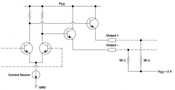
As we want to only use one cable to transmit information, the easy-phi external signals are uni-polar LVPECL. This means that the negative output of the LVPECL output stage shown above is directly terminated to Vcc-2V through a 50ohms resistor, while the positive one is terminated at the receiver's input. This particular standard has been chosen due to the availability of numerous receivers/transmitters and also because of its wide 0.8V differential voltage swing.
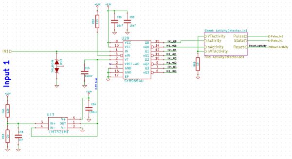
The HS Logic Gate board has 2 inputs, this is its input stage. Given that our signal is unipolar and that our receiver requires a differential one, we did some quick maths to implement an adaptation stage consisting of the R63 resistor (leave a comment if you want this detailed). Please note that U29 (a 1:4 LVPECL fanout) already integrates 2 termination resistors connected to the VT pin, where a simple op-amp based circuit provides the required Vcc - 2V = 0.5V.
Even if the Easy-phi project aims at producing great and cheap modules there is some functionality we need to add at each input that is quite costly: an activity detector.
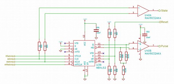
When experimenters build their setup, they always need to visually check that something is happening at one board's inputs. Our activity detector is therefore built around one fast D flip-flop and two comparators. The signal we want to monitor is fed to the flip-flop clock input, which triggers the acquisition of a logic 1. One of the two comparators then converts the LVPECL signal to a 3.3V unipolar one, which is sent to one of our microcontroller's inputs. Once the latter has seen the flip-flop output change, it resets the D flip-flop. Conversion from very low speed (<10Hz) cmos to lvpecl is done using 4 resistors (R95->R98).
In the NB4L52 flip flop, the (n)CLK input is connected to the (n)VTCLK pin through a 50ohms resistor. Instead of connecting VTCLK and nVTCLK to Vcc-2V (as per the specification) we usually take a 19ohms resistors instead, as the resulting voltage will hypothetically also be the same. The second comparator (on the top) allows us to monitor the signal state, in case the latter is extremely low speed.
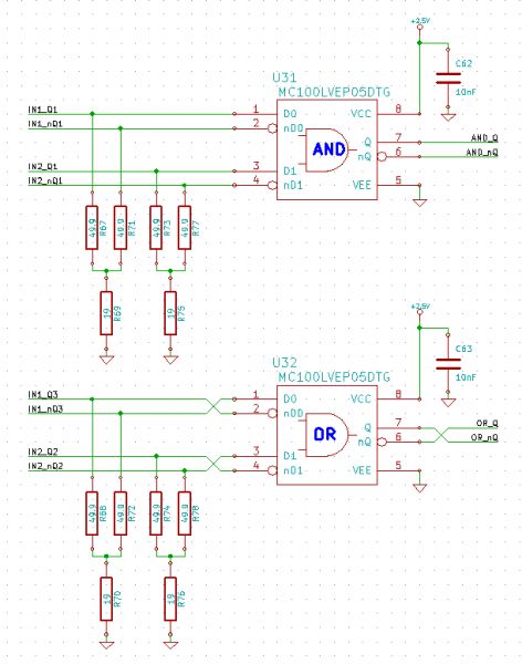
The 3GHz capable LVPECL OR/AND gates don't have termination resistors so we had to manually add them and use the 19ohms trick mentioned above.
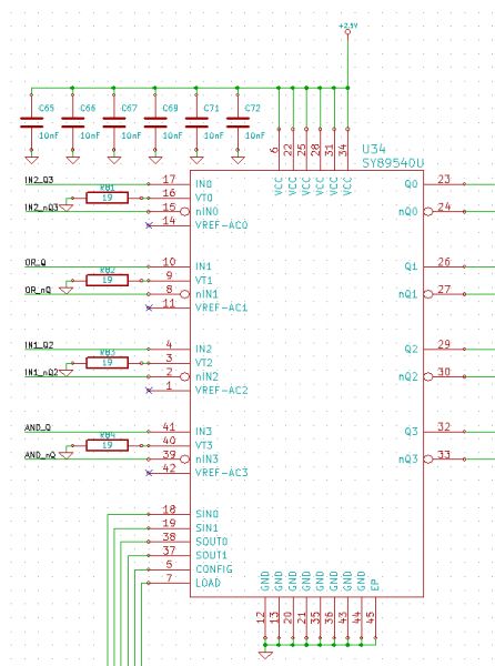
The IN1, IN2, OR & AND outputs are sent to a crosspoint switch. The latter is a simple programmable component that allows you to select which input should be sent to which output. It can receive LVPECL but outputs LVDS. Therefore, our HS Logic Gate module can also be configured as an Easy-phi signal fanout.
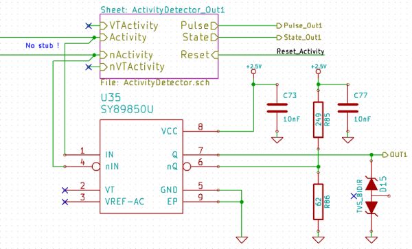
As we're implementing logic functions, we also need to visually monitor their output activity. However, very-fast differential signals are not meant to be received by multiple devices (here the activity monitor and the output stage) due to possible signal reflections that may occur. Still, an exception can be made when the receivers are physically very close to each other. The SY89850U from Micrel receives the crosspoint LVDS output and converts it to LVPECL. Its negative output is Thevenin terminated while its positve is sent to one output connector.
If you're still reading then let me congratulate you, as this was quite a deep look into high speed schematics! You're welcome to leave any question you may have, and you can contact the easy-phi team at easy-phi(at)unige(dot)ch. Here is a link to the official GitHub repository.

Comments
Might I suggest you to involve a proper microwave engineer to enhance your knowledge about RF layout fundamentals. In the text above you are worried about reflections, but the layout seems to suggest otherwise. A very basic thing would be to place ground via's near the transitions to another layer, to avoid mode conversions. I am not only taking about odd to even mode conversion, but also about parallel plate mode excitation.
Furthermore please perform some proper decoupling simulations, just throwing in a 10 nF seems a but high for these frequencies.
For a 2 GHz digital signal, the layout should at least be capable of handling frequencies up to 6 GHz (3rd harmonic), which seems a bit high, to just use your low frequency layout concepts. It might have worked for for this board, but with just a view RF-'tricks' you can improve the signal quality for future boards.