Amplifying nanosecond pulses for quantum physics experiments
By limpkin on Saturday, March 30 2013, 14:55 - My Projects - Permalink
Have no fear... even if this project sounds complex, you'll easily learn in this article many things about high speed electronics and PCBs.
In fact, my goal here is to teach you some basics about all the new problems that arise when you're dealing with GHz signals :-) .
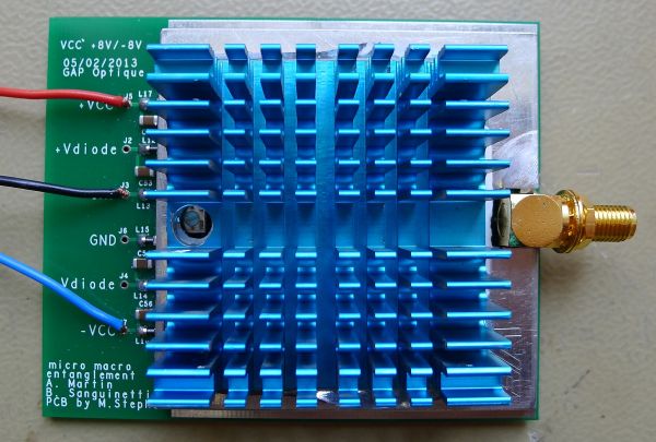
As you may have guessed, this is a work related project. Luckily, I didn't need to understand the quantum physics experiment my colleagues wanted to make in order to build this board :-D .
Anyway, to put things simply, this project consists in amplifying the measured light intensity difference between two photodiodes (both receiving less than nanosecond long pulses).
In my case, I chose to go for an operational amplifier (op-amp) based system (mainly for its ease of use), but FET based solutions would have worked as well (but they might have been more fragile).
Basic principles
First, a few things that we need to be aware of.
1) The output of a photodiode is a function of current. As we want the output of our amplifier to be a voltage, we actually need to make a transimpedence amplifier (alias a current to voltage amplifier).
2) Most high speed op-amp are using current feedback instead of conventional voltage feedback. Therefore, their inputs impedance are lower.
3) Most of the characteristics of an op-amp will vary depending on the gain you set.
4) As we are dealing with pulses, the most important parameter of the op-amp you need to look at is its rise/fall time rather than its bandwidth.
Design choices
You may ask: how can an op-amp have a "slower" rise time than its 1/3*bandwidth?
Well my guess it that the fourrier transform of the fastest signal rise contains higher frequency components than ~3 times its rise/fall time (up->down->up) due to its gaussian-like shape. This may not be true with tiny output signals.
Anyway, the best op-amp I found out there at the time was the THS3202 from Texas Instruments so I went for it.
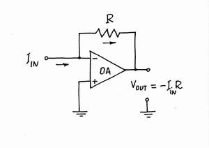
However, as it is a current-feedback operational amplifier, we had to take care of its inputs impedances which are quite low.
Therefore, this conventional op-amp based transimpedance amplifier wasn't possible:
 Moreover, as we needed a total gain of at least 100, because of the previously explained reasons, I had no other choice than to cascade three op-amps, each one of them having a 5x gain, adding up to a total 125x gain.
The schematics
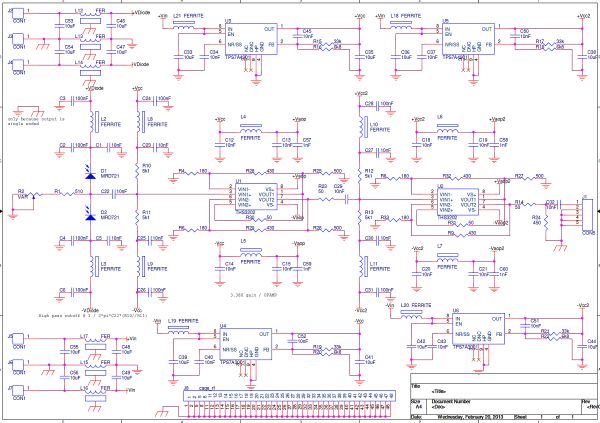
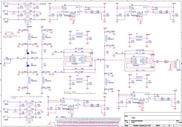 Don't be overwhelmed ;-) .
As the voltage variation we want to measure (at the node between D1 and D2) is around 1 mV, parasite filtering is the key here.
Here are all the techniques used:
- ferrites are chosen to filter all the DC voltages going to key components (diodes, op-amps, re-biasing stages), with decoupling caps before and after them. These ferrites should be RF specified, as we'll need a high impedance at high frequencies.
- to filter the input DC voltages, L12->L17 actually are dedicated LC filters that have a third pin that needs to be grounded.
- we used very low noise LDOs instead of step-downs to avoid the switching noise to be introduced in the rest of our system
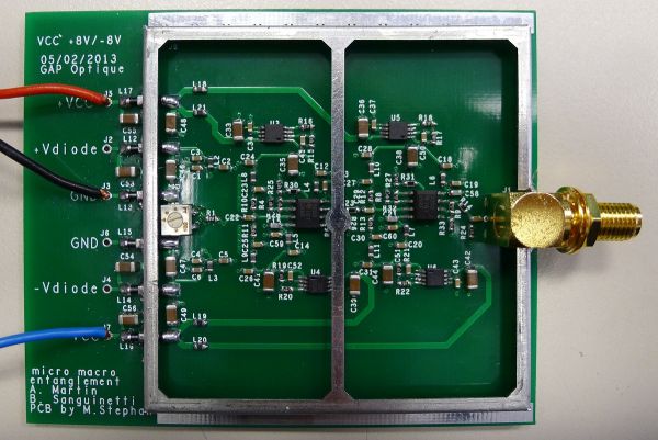
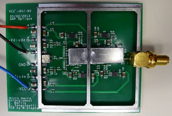
- we bought a shielding cabinet that will be placed on top of the PCB to shield it from RF signals. It should be connected to the shielding ground.
- (in an ideal case) the ground inside the cabinet should be connected through a single connection to it (and therfore to the ground outside the cabinet).
The reason for the last point is that we should provide a single shielded ground to all the sensitive components. It should be a non-perturbated reference for all of them.
However, because our ouput is single ended, the signal is coming back through the cable shielding. Therefore, the ground on the connector needs to be the same as the op-amp's.
If the output had been differential (one coax for the signal, another for the return), then the cables shielding and connector ground would be connected to the cabinet's outside ground. The signal ground would only be present in a tiny space (inside the cabinet) shielded from possible perturbations.
 A few words about the signal path.
In these schematics, the transimpedance stage is made using a simple variable resistor connected to the ground. At the node, we are AC coupled with the positive input of our operational amplifier and a rebiasing stage.
This has the main advantage of (if we wanted) to have different grounds for the diodes and the opamps. Moreover, as the choice of the opamp feedback resistors is dictated by its datasheet, we can get a relatively high impedance at the node, as we don't need to connect the node to the negative input of our opamp, as a normal transimpedance amplifier would need.
You'll also see a second rebiasing stage, as the biasing voltage at R10/R11 may not be exactly 0V (due to the input bias current of the opamp) and therefore could be amplified by 25.
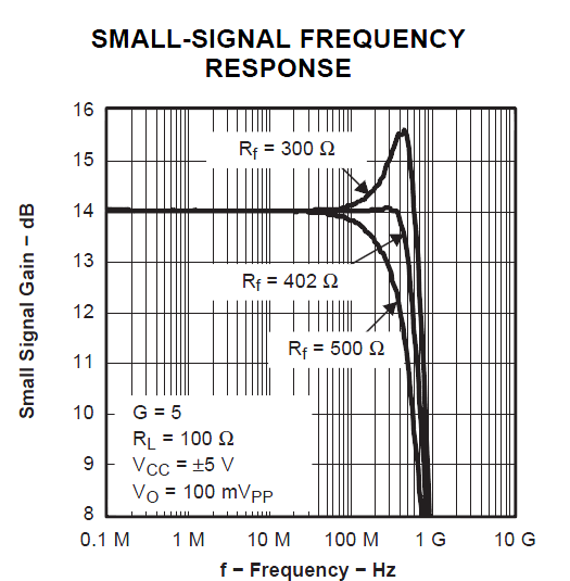
You can see in this graph that depending on the feedback resistor, you actually can amplify the high frequency components of your signal, which was quite convenient in my case.
Again, follow the guidelines of the op-amp datasheet, as you can't really use any resistor value you want under penalty of having an unstable circuit.
To be sure of our bandwidth, I made a low pass filter using a capacitor in parallel with the feedback resistor. However, resistors have a parasitic capacitance of ~0.2pF so you need to take this into account.
Parasitic capacitance is our biggest enemy. As we are dealing with GHz signals, you'll need to put a small resistor in series with the opamp output. Otherwise, it'd be like the opamp was driving a (parasite) capacitor, which can generate a high frequency ringing.
The rest of the circuit is pretty much straight forward. There are two LDOs for each + or - Vcc simply because one can't provide enough current for two op-amps.
The schematics - version 2
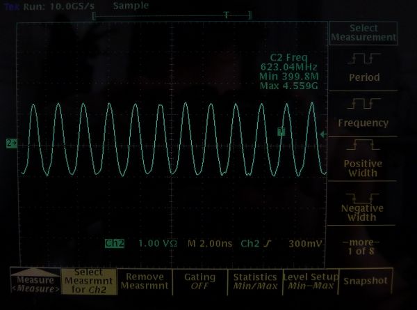
As it turns out, when testing the PCB the first op-amp was oscillating by itself at 550MHz.
One of the reasons I thought of was that setting so much gain on the amplifier created a positive feedback on the power supply.
Because there's a load at the output of the op-amp (which is +/- required for a current feedback op-amp), any oscillation creates a load on the power supply and therefore a drop in voltage, which can be amplified by the operational amplifier if the power supply rejection ratio is not high enough. Here is a very interesting article about that.
The solution I thought at the time was therefore to spread the gain over the 4 op-amps.
The guys at texas instruments also provided me with some useful advices:
The most likely cause for the ringing you observe would be the light compensation of the THS3202 in a gain of +5V/V. The datasheet, figure 10 & 11, shows ~2dB of peaking for 340ohm in the feedback resistance. The capacitor across the feedback resistors, C8, C10 & C16 may help flatening the response, but in general it is not a recommended implementation for a current feedback amplifier as it may destabilize it. The first THS3202 is likely to exhibit the problem more as there are 2 stages with the same peaking adding the overall peaking for that stage. I would recommend removing C8, C10 and C16 and increasing the feedback resistances to 420ohm. Rg would then be 105ohm. I notice the output of Amp A directly feeds into the + input of Amp B on both stages. In theory this is fine as the + input is high impedance. However, the input does have capacitances associated with it which can impact high frequency stability of the driver amp. It is recommended to place a 49.9-ohm resistor in series on each output to + input.
which lead to the second version of the schematics:
You'll also notice that I added another decoupling 1nF capacitor to the opamps (better suited for higher frequencies), and also 500ohms loads on each op-amp. Adding the extra capacitor will also prevent our main capacitor from behaving like an oscillator (yes... this happens!).
The "schematics" - version 3
As it turns out, when receiving the second version of my PCB the ringing was still present (damn it!).
However, I found the problem in less than an hour: the max quiescent current of one op-amp channel is so high that the THS3202 will get quite hot and then start to oscillate by itself (I love cold sprays!).
To give you some numbers, as I'm using +7/-7V to power the op-amps and the max quiescent current of one channel is 21mA, the total power that needs to be dissipated is therefore 14*0.021*2 = 0.588W. This is quite a lot for a SOIC package that doesn't have good package dissipation ratings. I therefore had to add a homemade heatsink on the op-amps.
The PCB
When routing a circuit board containing high speed signals, there are a few rules to follow:
- keep traces (very) short
- have an uninterrupted ground (and power) plane in one of the layers
- try to keep power supplies away from analog signals
- have a "natural signal flow" from the source of the signal to the end (quite subjective right?): no sharp turns, etc etc
For long traces, depending on your components, you may need to design 50ohms traces (there are many calculators online for that) to be sure that all the transmitted power is correctly absorbed and not reflected.
When routing, you should imagine that all your traces are inductors. Therefore, in a two layers setup, Vcc should respect this path: Vcc -> decoupling cap's pin -> component's pin.
The assembly
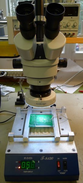
As there is an uninterrupted ground plane on the bottom layer, the thermal inertia of the PCB is quite huge.
If you're doing the same kind of PCBs, I advise you to buy a pre-heating station to heat your PCB to 60° celsius so soldering will be easier ;-) .
The cooling
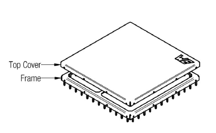
As previously mentioned, the THS3202 will get so hot that it will start ringing by itself. I therefore made a heatsink to make the SOIC <> cabinet contact.
And on top of the cabinet, I added another heatsink:
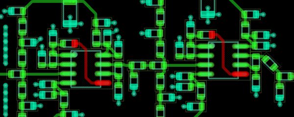
The reason why I chose the THS3202 in a SOIC package instead of MSOP (that has a heatpad) is that I didn't want to interrupt the ground plane to cascade the two op-amps in the chip.
As there is no heatpad, the trace connecting the two op-amps is under the chip (red traces):
For future versions we will use a 4 layers PCB and the THS3202 in the MSOP package, especially now that seeedstudio has a 4 layers service. The heat will therefore be directly dissipated in the ground plane and we won't need all these fancy heatsinks.
The cooling V2
Well, it turns out that this cooling "sandwich" was not optimal and that the THS3202 would also oscillate (damn it! bis).
This is mainly explained by the fact that the cabinet is not a good thermal conductor and also because there is a big temperature difference between the die inside the SOIC and the top of the package (called junction temperature).
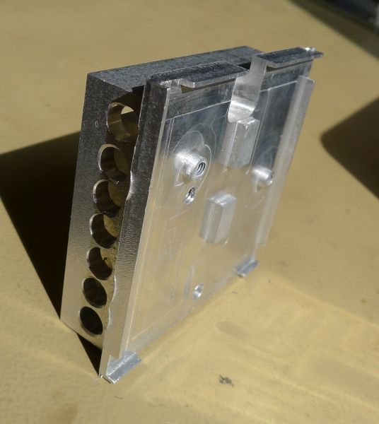
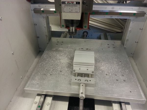
I therefore lowered the supply voltage to +5/-5V, found an aluminium 2cm plate and used my favorite CNC:
The fancy box
As mentioned in the title, this PCB will be used by physicists. I therefore needed to make a "fancy" enclosure to protect the circuit from what may happen.
I actually adapted my PCB outline dimensions so it could fit in a box I had found on digikey. This particular box had grooves on the inside ;-) .
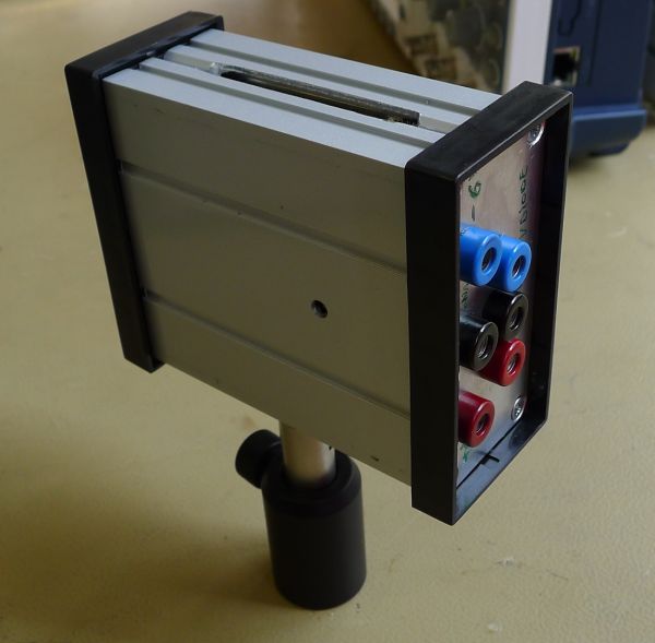
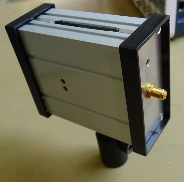
I then just needed to machinate the different openings:
to get this final result:
Final rise time
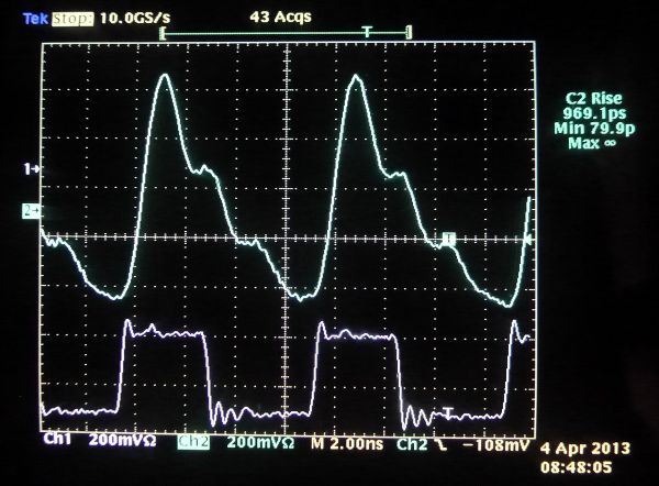
Finally, we set up our experiment table and looked at our rise time:
If you look at the top trace, we measured in average around 950ps, which is not bad at all :-) ;

Comments
Thank you so much for this blog. I really enjoy reading it and I gain a lot from it. Thank you!
@jdb78 : Thanks! You are welcome :-)
Which LC filters did you use?
Also which ferrites did you chose? I'm trying to implement an EMI circuit for an amplifier design with similar bandwidth requirements are the one you designed.
@Andrei : Hey Andrei,
LC filters: NFE61PT472C1H9L and i'll get back to you for the ferrites :)
Very helpful thanks. Would you consider the AD8009 for this type of application?
@IanD : unfortunately it doesn't have the same performances as the one I used :)